free website hit counters
Get a free website hit counter here.

Intel introdcued new Atom Brand for Low-Power Processors  

Wednesday, June 17, 2009


The Intel® Atom™ processor will be the name for a new family of low-power processors designed specifically for mobile Internet devices (MIDs) and a new class of simple and affordable Internet-centric computers arriving later this year. Together, these new market segments represent a significant new opportunity to grow the overall market for Intel silicon, using the Intel Atom processor as the foundation. The company also announced the Intel® Centrino® Atom™ processor technology brand for MID platforms, consisting of multiple chips that enable the best Internet experience in a pocketable device.

The Intel Atom processor is based on an entirely new microarchitecture designed specifically for small devices and low power, while maintaining the Intel® Core™ 2 Duo instruction set compatibility consumers are accustomed to when using a standard PC and the Internet. The design also includes support for multiple threads for better performance and increased system responsiveness. All of this on a chip that measures less than 25 mm², making it Intel’s smallest and lowest power processor yet.1 Up to 11 Intel Atom processor die — the tiny slivers of silicon packed with 47 million transistors each — would fit in an area the size of an American penny.

These new chips, previously codenamed Silverthorne and Diamondville, will be manufactured on Intel’s industry-leading 45nm process with hi-k metal gate technology. The chips have a thermal design power (TDP) specification in 0.6-2.5 watt range and scale to 1.8GHz speeds depending on customer need. By comparison, today’s mainstream mobile Core 2 Duo processors have a TDP in the 35-watt range.

“This is our smallest processor built with the world’s smallest transistors,” said Intel Executive Vice President and Chief Sales and Marketing Officer Sean Maloney. “This small wonder is a fundamental new shift in design, small yet powerful enough to enable a big Internet experience on these new devices. We believe it will unleash new innovation across the industry.”

With personal computing increasingly going mobile and the computer industry rapidly developing new classes of products to connect the next billion people to the Internet, the Intel Atom processor offers customers the unique ability to innovate around the new low-power design. In addition to the MID opportunity, Intel believes the demand for a new category of low-cost, Internet-centric mobile computing devices dubbed “netbooks” and basic Internet-centric desktop PCs dubbed “nettops,” will grow substantially over the next several years. The Intel Atom processor is perfectly suited to meet these new market segments.

Intel said the Intel Atom processor also has potential for future revenue opportunities in consumer electronic devices, embedded applications and thin clients.

Intel Centrino Atom Processor Technology
The Intel Centrino Atom processor technology brand represents Intel’s best technology for MIDs. Formerly codenamed “Menlow,” Intel Centrino Atom processor technology includes the Intel Atom processor, a low-power companion chip with integrated graphics, a wireless radio, and thinner and lighter designs. Together, these components are designed to enable the best mobile computing and Internet experience on these new devices.

Chip - RCA 1802 Microprocessor chip (1974)  


The 1802 was RCA's first single chip CPU and was a peer to the Intel 8080. The 1802 was used in the COSMAC microcomputer kit and a space hardened versions were the brains for the Voyager, Viking, and Galileo Spacecraft. It had sixteen 16-bit registers, which could be accessed as thirty-two 8 bit registers.


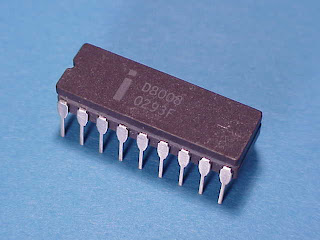
The Intel 8008 was a microprocessor intended for use as a terminal controller, and was similar to the Intel 4040. The 8008 was the first 8-bit microprocessor. The 8008 was originally code named the 1201. The 8008 had a 14-bit PC and addressing and an eight level internal stack. The 8008 was a very important transition CPU for Intel Corporation. The work on the 8008 really enabled the creation of the powerful 8080. This chip is a Dual Inline Package (DIP) made of gray ceramic and tin pins. The 8008 contained 29,000 transistors.

Chip - Intel P4004 Microprocessor (1969)  


Shown is the historic Intel P4004 microprocessor. The 4004 is considered the world's first microprocessor. The 4004 was created by Intel with Ted Hoff and Federico Faggin as the lead designers. The 4004 provided a new tool to the world. Up to that time and semiconductors and IC's ("integrated circuits") were built for a specific purpose. The 4004 was the first semiconductor device that provided, at the chip level, the functions of a computer. Although the 4004 was created for use in calculators, it was found to have many other applications.

The Intel 4004 provided the basic building blocks that are still found in today's microcomputers: the arithmetic and logic unit and the control unit. The 4-bit Intel 4004 ran at a clock speed of 108 kHz and contained 2,300 transistors. The 4004 processed data in 4 bits, but its instructions were 8 bits long. The 4004 could address up to 1 Kb of program memory and up to 4 Kb of data memory. The 4004 chip had sixteen 4-bit (or eight 8-bit) general purpose registers, and an instruction set containing 46 instructions. The packaging design of the P4004 was plastic with tin pins in a DIP ("Dual Inline Package") configuration.


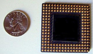
In 1993, Intel announced the Pentium chip. The word "Pentium" comes from the Greek root word "pentas" meaning "five." The Pentium is the Intel 80586 chip. The Pentium is a 32-bit chip with superscalar design, and is estimated to be two times faster than the 486DX2 (66MHz) chip. The Pentium uses dual pipelines to allow it to process two separate instructions in a single cycle. The Pentium has a 64 bit bus interface, an eight bit code cache, an eight bit data cache, and branch prediction memory bank. Don Alpert was the architecture manager of the Pentium, John Crawford was co-manager. In March 1994, Intel announced new and faster versions of the Pentium microprocessor, with speeds of over 100 MHz. By 1996, 200 Mhz microcomputer systems were available on the market. (This chip has now been far surpassed by current microprocessor technology.)

Intel 80586 Chip (Pentium) 1993  


In 1993, Intel announced the Pentium chip. The word "Pentium" comes from the Greek root word "pentas" meaning "five." The Pentium is the Intel 80586 chip. The Pentium is a 32-bit chip with superscalar design, and is estimated to be two times faster than the 486DX2 (66MHz) chip. The Pentium uses dual pipelines to allow it to process two separate instructions in a single cycle. The Pentium has a 64 bit bus interface, an eight bit code cache, an eight bit data cache, and branch prediction memory bank. Don Alpert was the architecture manager of the Pentium, John Crawford was co-manager. In March 1994, Intel announced new and faster versions of the Pentium microprocessor, with speeds of over 100 MHz. By 1996, 200 Mhz microcomputer systems were available on the market. (This chip has now been far surpassed by current microprocessor technology.)

The Core 2 Extreme QX9650 Processor  


The Core 2 Extreme QX9650 is a Yorkfield quad core processor, featuring dual 6MB of independent L2 cache, for a total of 12MB of Advanced Smart Cache. This doesn't change the current Intel quad core design used with Kentsfield, and the 45nm Yorkfield is still a pair of Wolfdale dual cores on a single processor package. The processor supports the LGA775 package, runs at a core speed of 3.0 GHz, and uses a bus speed of 1333 MHz.


It also supports basic features like Intel Virtualization Technology, Execute Disable Bit, Intel 64 architecture, and SpeedStep. Although this is a 45nm processor running at a default core voltage of 1.1-1.2V, Intel still uses a 130W TDP. Motherboard support is also a potential bright spot, as most 1333 MHz platforms should handle a 45nm Penryn with a BIOS update, and there is even *unofficial* Penryn 1333 MHz support on older boards from companies like ASUS. Check your motherboard vendor website just to be sure.

The only real surprise is the 3.0 GHz clock speed. Launching a new processor line at a clock speed that has already been reached is kind of anticlimactic. After all, Intel already has the 3.0 GHz Core 2 Extreme QX6850 quad core, and now we get another 3.0 GHz quad core, albeit at 45nm. This is surely a response to AMD and their nonexistent challenge at the top-end of the processor market


Intel Core 2 Extreme QX9650 Review
By Vince Freeman : October 29, 2007 


Introduction

There are a couple of tried-and-true strategies of the PC world that never seem to get old, and continue to supply us with endless new processor revisions and ever-higher performance. One of these is the venerable die shrink, where process technology moves to the next level, allowing ever-smaller transistors, and potentially higher clock speeds. This does not represent a new architecture, but an enhancement on the existing one, and in the process, extends its lifespan. We've seen this employed in virtually every processor line, and now it's time for the Core 2 to get a facelift, moving from 65nm to a new 45nm world. 

The 45nm Penryn Explained

The Intel Penryn is the name given to Intel's 45nm processor family, which is made up of the Yorkfield quad core and Wolfdale dual core models, which correspond to the Conroe (dual) and Kentsfield (quad) from the 65nm era. Both Penryn models are based on 45-nanometer (nm) High-k metal gate silicon technology, which uses a combination of high-k gate dielectrics and conductors, rather than silicon, to build the transistor gates in a Yorkfield quad core. A prime advantage of this technology is faster transistor switching speeds, but at reduced power, which in turn allows higher processor speeds at a lower thermal and power envelope.

Another bonus to any die shrink is that the basic core architecture has been tweaked and improved since inception, and the Penryn will include the latest microarchitecture enhancements. Other enhancements include SSE4, Super Shuffle Engine, Enhanced Intel Virtualization Technology, and Fast Radix-16 Divider. This last feature effectively doubles the divide speed of the Penryn compared to previous models, which can aid in the performance of any math intensive functions. Power efficiency is also addressed through features like Deep Power Down Technology, which improves on the 65nm Core 2 by allowing, according to Intel, the lowest power state a processor can reach.


Lower power consumption  


Power consumption has been a big issue in Yonah's creation. A lot of attention has been paid to the leakage current -- the power taken when the chip isn't doing any processing at all. Although this is typically a few billionths of a watt per transistor, with 151 million transistors it becomes a major issue. Various techniques can improve the situation, such as switching off power altogether to idle areas of the chip and changing the transistor geometry and composition to improve the insulation between its components. Intel says that it's now designing for power consumption in the same way that it has always designed for minimal chip area and most effective timing, but that deciding to do this came about almost by accident: it found big power advantages while designing for aggressive area reduction just as the market started to worry about watts.

The cores themselves have a complex series of power saving options: Active, Halt, Clock Stopped, Sleep, Deeper Sleep and Enhanced Deeper Sleep, which successively push the chip deeper into a coma from which it takes successively longer to return. Each core can slip into the appropriate mode independently of the other; dynamic power management also watches the frequency and power trade-offs for portions of the cores. The cores can finesse their frequencies as appropriate, but don't have independent voltage control; Intel says it looked at this, but that the form factors for multiple off-chip voltage regulators and the complications caused by routing split high-quality power feeds across the circuit board made this an unappetising option.

Off-chip factors haven't been ignored. More precise thermal monitoring of hotspots on the chip should mean that power isn't wasted spinning the cooling fan before it's needed. The chipset can also be safely powered down when the CPU is asleep through a process rather cutely called Dynamic Bus Parking. The chipset itself can abandon main memory to self-refresh mode during enhanced deeper sleep; it can minimise the amount of memory accessed by the display, dim the backlight automatically and compensate by lightening the LCD's pixels, and read an external sensor to reduce the brightness when the computer is being used in low light levels.

Cleverer cache
Back in the CPU, the Level 2 cache is a major part of Yonah's design. The 2MB of L2 cache is dynamically allocated between the two cores -- the busier core gets more cache. If one core is idle, the whole of the L2 cache becomes available to the other; if both cores are idle, then the cache can go into one of a number of sleep modes, including one where some or all of the data is written out to main memory and some or all of the cache is physically turned off. Improvements to the caching algorithms and deeper write buffers also reduce expensive main bus traffic, which would otherwise reduce performance and increase power consumption.

Both cores share a single bus into the cache, and data that's shared between processes on different cores can be accessed by either core without creating main bus traffic. This is unlikely to be much of an issue in typical notebook use, but is an example of an architectural feature that may become more important as the chip design filters into servers. It also compensates somewhat for the lack of a dedicated interprocessor bus.

The Core Duo processor's 2MB of Level 2 cache is dynamically allocated between the two CPU cores, which share a single bus into the cache.

Yonah has some good old-fashioned logic and arithmetic improvements too. It can bundle more instructions together for simultaneous handling -- both ordinary and SSE multimedia -- and do some operations in one micro-op that took four before. It's got deeper pipelining in the floating-point multipliers and more intelligent integer dividers that can do 32-by-32-bit divides in between a half and a quarter of the cycles required by the previous chip. Intel says that software profiling suggests that a lot of divisions will be helped by this: it might be a peculiarly obscure part of the chip's design, but the engineers are rather proud of it. Finally, there are more integer arithmetic units and ten new SSE3 instructions for media handling. In all, a fairly respectable smorgasbord of minor novelties that should lift overall performance across the board.

Yonah's designers are keen to emphasise that dual-core fits neatly into the hyperthreading story, but with higher performance than hyperthreaded chips because both threads are entirely independent. However, most of the headline performance issues with hyperthreading have been cache issues, where a wide-ranging housekeeping thread skips through large amounts of main memory to the extreme detriment of other processes. Dual core by itself doesn't help here: it could be that the improved dynamic cache allocation logic in Yonah will lead to fewer severe conflicts, but that remains to be seen

Outlook
Intel claims that the third quarter of 2006 will see two major events: the point at which dual core shipments overtake over single core, and the point at which 65nm achieves parity with 90nm. Mobile processor shipments are also increasing rapidly after languishing at around 20 percent of all processors: growth kicked off in Q2 of 2004 and is now at around 33 percent with 'not long' to go before 50 percent is reached, according to Dadi Perlmutter, general manager of Intel's mobility division, when he talked to CNET.com.au sister site ZDNet UK. He also said that the company is 'at least three quarters ahead of the competition' in 65nm, and 'one to two quarters ahead' in dual core on mobile platforms.

Inside Intel's Napa platform  


Intel's latest mobile platform, now officially christened Centrino Duo, introduces the Core Duo (Yonah) chip with dual CPU cores. This and other developments should deliver useful -- if not revolutionary -- increases in notebook performance and battery life.

The launch of Intel's new Napa platform brings with it Yonah, the company's first dual-core mobile processor. Now more properly named the Intel Core Duo, Yonah is an evolution of the Pentium M processor. As it's also expected to find its way into low-power blade servers and the like, there's no M or Mobile in the processor name: the next generation of this architecture, codenamed Merom, will move further into full-blown desktop (Conroe) and server (Woodcrest) configurations.

Core facts
Intel's nomenclature takes a bit of work to decode. The Napa platform is officially called Centrino Duo, which includes the Mobile Intel 945 Express chipset, the Intel PRO/Wireless 3945ABG Wi-Fi PCI Express MiniCard and the Intel Core Duo processor. A low-cost version of the platform built around a single-core Yonah -- why throw away a faulty chip if only half has failed? -- is simply called Centrino as before, although the processor chip itself is labelled the Intel Core Solo.

Intel's new Centrino Duo mobile platform (previously codenamed Napa) comprises the Core Duo (Yonah) processor, the PRO/Wireless 3945ABG wireless networking module and the 945 Express chipset.

Yonah's two cores are functionally identical mirror images of each other, which simplifies the routing of common signals between them. Apart from duality, Yonah's biggest -- or smallest -- change is its architectural feature size, shrunk to 65nm from its predecessor Dothan's 90nm. This smaller size keeps the processor line in track with the precepts of Moore's Law, and gives the designers more room to trade off performance against power consumption. Intel claims that Yonah has twice and Merom will have three times the integer performance per watt of Banias, the 130nm mobile chip that kicked off this line of designs.


How many people cloud say why 1959 is an important date ? Probably not many .But this the year when the chip was invented. You may then ask , " But what is a chip?! " It is the nickname for a small piece of silicon that, like magic, is changing modern life. This chip which under microscope looks like a city map of streets and buildings , is an integrated circuit, the " brain " in our computers, calculators, watches and other electronic goods that save time and labor and help us work with greater precision . 
 
Many uses were soon found for the new invention , and scientists made chips that were more and more complicated. Computers ,which were once so big and expensive, could now be smaller and cheaper. People could have their own personal computers and use them in their homes. Chips went into television sets, radios, car engines. In a popular video game the chip may take a player into space to fight imaginary battles, or in a fast car down a busy highway where there are many dangers. When we buy things in a shop that has an electronic cash register, the clerk just passes the articles we have bought over a certain spot, and the computer gives the price of each article , then adds them up , and finally corrects the shop's records of how much it has of each article. 
 
The place in California where this new industry originally developed got its nickname, Silicon Valley, from the material that is used to make the chip.Silicon Valley is near two well-known universities ( Stanford and Berkeley ) ,and it is interesting that ii is not far from the place where gold was discovered in 1849, which also brought thousands of people to California. This time people who came were scientists and engineers !

Intel Centrino 2 Processor Technology for Laptop Computers  

Intel’s BEST performing laptop technology includes:
• Up to 50% faster performance when multitasking‡1
• Optimized for wireless—up to 2X greater range and up to 5X better Wi-Fi performance, with optional built-in WiMAX to equip your laptop for the future of metro-wide broadband wirelessΔ2 Δ3
• Designed for the longest possible battery life
• Up to 90% faster performance on intensive multi-

media applications like HD video encodingΔ4

About intel

Intel pushes the boundaries of innovation so our work can make people's lives more exciting, fulfilling, and manageable. And our work never stops. We never stop looking for the next leap ahead—in technology, education, culture, manufacturing, and social responsibility. And we never stop striving to deliver solutions with greater benefits for everyone

Design by Amanda @ Blogger Buster